

reduce EMI in Pcb productions
Electromagnetic interference (EMI) is a common concern in PCB production, particularly as devices become more compact and electronics operate at higher frequencies. EMI refers to the unwanted noise or interference that can be emitted from an electronic circuit, potentially disrupting the performance of nearby components or even entire systems. To ensure the efficient operation of electronic devices, it is crucial to manage and reduce EMI in PCB productions. There are several strategies and best practices that designers and manufacturers can employ to mitigate EMI in PCBs, ensuring that the final product is both reliable and compliant with electromagnetic compatibility (EMC) standards.
One of the most effective methods of reducing EMI in pcb production is implementing a robust grounding system. A solid ground plane provides a low-impedance return path for signals and helps reduce the potential for EMI. By placing a continuous ground plane on the PCB, usually on an inner layer in multi-layer boards, you can minimize the loop areas where current flows, thus reducing the chances of electromagnetic radiation. A solid ground plane also prevents noise from propagating into sensitive areas of the circuit, offering a shield against external electromagnetic disturbances.
Another powerful approach to reducing EMI in PCB production is using shielding. Shielding involves enclosing the circuit or parts of the PCB with conductive materials to block or absorb electromagnetic waves. Designers can use metal enclosures or copper shielding around high-frequency components to prevent EMI from escaping or entering the PCB. Additionally, shielding vias are used to connect the shield to the ground plane, ensuring that any trapped EMI is safely diverted to ground instead of radiating outward. Shielding can be particularly important in high-frequency circuits, such as those found in wireless communication systems and RF (Radio Frequency) devices.
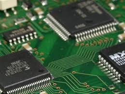
How do you reduce EMI in Pcb productions?
Controlling impedance is another key strategy for reducing EMI in PCB production. Impedance mismatches between transmission lines, connectors, and other components can cause signal reflections, leading to noise generation. By designing traces with controlled impedance—usually 50 ohms or 75 ohms—PCB manufacturers can ensure that signals travel efficiently and without generating unwanted electromagnetic interference. This is particularly critical in high-speed and RF circuits. Impedance control involves selecting the correct trace width and ensuring that traces are routed with proper spacing from the ground plane, which minimizes signal integrity issues and reduces EMI.
Crosstalk, or the unintentional coupling of signals between adjacent traces, is another source of EMI. To reduce crosstalk in PCB production, designers can increase the spacing between high-speed signal traces, separate sensitive signal lines from noisy power traces, and use differential pairs for high-speed signals. Differential pairs are pairs of traces that carry complementary signals, reducing noise and minimizing EMI. Additionally, placing traces at right angles and avoiding parallel routing for long distances can significantly reduce the likelihood of crosstalk and its associated interference.
Decoupling capacitors play a crucial role in managing noise and reducing EMI in PCB production. These capacitors are strategically placed near power pins of active components to filter out high-frequency noise from the power supply. They act as local energy reservoirs, providing a stable voltage and reducing fluctuations that could lead to EMI. When designing PCBs, it is essential to use capacitors with appropriate values for the frequencies being filtered and to place them as close as possible to the components they are protecting.
The placement of components and the routing of traces significantly impact EMI. Placing high-speed or high-power components away from sensitive areas, such as analog circuits or RF components, helps to reduce the risk of interference. Traces should also be routed in a way that minimizes the loop areas and avoids crossing noisy power traces with sensitive signal traces. Careful planning of the PCB layout helps to avoid generating or amplifying EMI.
In conclusion, reducing EMI in PCB production requires a multi-faceted approach that includes proper grounding, shielding, impedance control, minimizing crosstalk, and thoughtful component placement. By implementing these techniques during the design and manufacturing stages, PCB designers can create circuits that meet EMC standards, ensuring optimal performance and minimal interference in sensitive electronic systems. As electronic devices continue to evolve and operate at higher frequencies, reducing EMI will remain a critical aspect of PCB production to ensure the reliability and compliance of modern electronics.